CEA-Leti and STMicroelectronics presented research findings at IEDM 2025 detailing key enablers for a new high-performance and versatile RF Silicon platform. The joint work focuses on co-integrating best-in-class active and passive devices used in RF and Optical Front-End Modules (FEM).
The paper, titled “Unlocking High-Performance Si RF Platforms with SiGe HBT and RFSOI Switch Technologies,” outlines the 3D sequential integration of silicon-germanium (SiGe) heterojunction bipolar transistors (HBT), RF SOI switches, and high-quality passives on a single wafer. This approach opens a path toward highly integrated, low-parasitic, and cost-efficient systems for next-generation wireless and wireline communications.
Instead of being packaged or stacked as separate chips, these high-performance components can be built directly onto the same silicon wafer. 3D sequential integration allows for the layering of different device types, such as SiGe HBT and SOI CMOS switches, without the processing steps overheating the lower layers.
“Our team has shown that high-performance SiGe HBT has been conceived to be compatible with the top-tier fabrication steps, and that trap-rich isolation can be localized and thermally robust, and low-temperature (600°C) SOI switches can match state-of-the-art figures of merits,” said CEA-Leti’s Thibaud Fache, lead author of the paper. Fache added, “These results pave the way to an all-silicon RF front-end module that is efficient and cost-effective.”
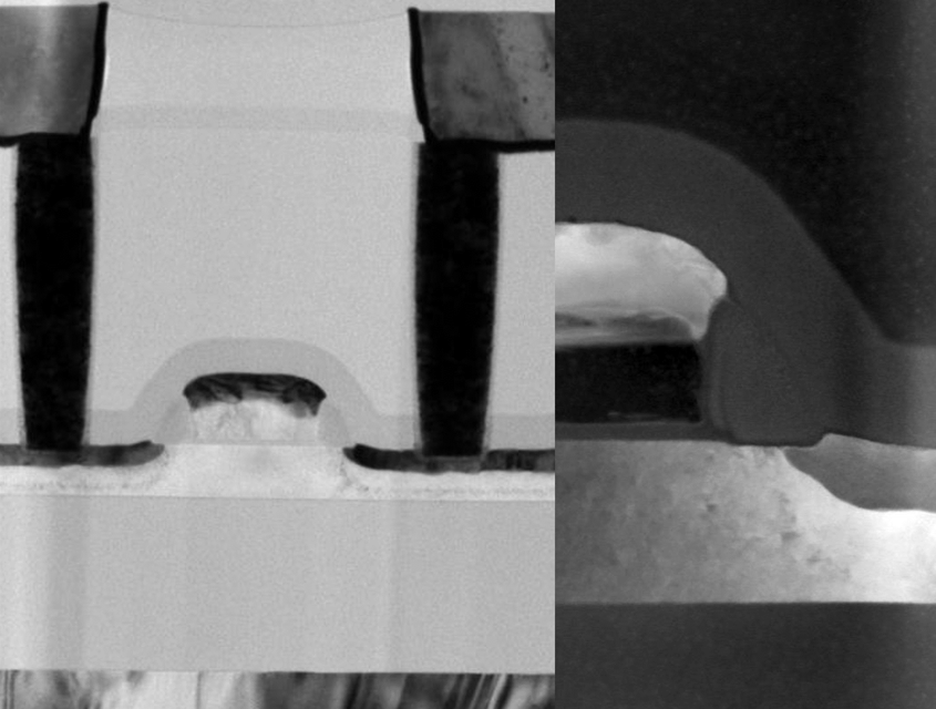
The researchers demonstrated that a localized trap-rich layer could achieve RF isolation and linearity comparable to expensive commercial trap-rich substrates. Crucially, this layer can withstand thermal cycles up to 600°C, which preserves the performance of the underlying SiGe HBT layer.A materials science milestone noted in the research is achieving a performant RF Partially Depleted (PD) SOI switch at 600°C, contrasting with the standard process temperature of approximately 1000°C.
The process flow for this low-temperature device does not require new equipment or costly steps, which makes it quickly industrially viable due to the relatively relaxed 600°C thermal budget constraints of the bottom tier.
The team confirmed the feasibility of a fully integrated silicon RF platform by demonstrating high-quality, low-loss RF switches fabricated at 600°C while maintaining the performance of the SiGe HBT underneath.
The work, by extending silicon’s sequential integration capabilities into the RF domain, points to a future of more accessible, energy-efficient connectivity. Fully integrated RF and optical front ends could simplify manufacturing and enable the cost-effective deployment of dense wireless networks, which are essential for smart cities, autonomous systems, and AI datacenters.
“This joint result demonstrates a credible path from advanced research to manufacturable solutions,” said ST’s Thomas Bordignon, co-author of the paper. Bordignon stated that by combining CEA-Leti’s sequential integration know-how with ST’s RF technology expertise, they are “enabling the co-integration of state-of-the-art SiGe HBT, switches and passive devices, that are key elements of the FEM.”
In an additional presentation, CEA-Leti researchers reported a breakthrough in designing high-performance silicon-on-insulator (SOI) MOSFETs processed at 400°C. These NMOS and pMOS transistors are stated to show state-of-the-art performance among Back-End-Of-Line devices, fulfilling all industrial figures of merit without compromise. This reliable versatile analog transistor targets More Than Moore applications, bringing differential advantage for smart sensors, near memory computing and RF devices.