Carrier boards are the architectural cornerstone of modern embedded systems. They provide the vital link between high-performance compute modules and the rugged, application-specific demands of the real world. By decoupling the fast-moving processor roadmap from slower-moving hardware interfaces, engineering teams can extend product lifecycles, simplify AI acceleration upgrades, and reduce the risks associated with total system redesigns.
This guide explores the technical nuances of carrier board design, from signal integrity and power sequencing to the mechanical and thermal constraints that define a production-ready platform.
Defining the Carrier Board Architecture
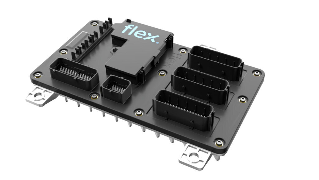
In professional embedded engineering, a carrier board is a specialized PCB designed to host a System-on-Module (SOM) or Computer-on-Module (COM). While the module acts as the “brain,” the carrier board serves as the “nervous system,” providing the physical interfaces, power regulation, and protection circuitry required for a specific deployment.
Distinguishing the Hardware Layers
Terminology in the embedded space can be fluid, but the functional distinctions are critical for specification:
- Carrier Board: An application-specific board that mates with a SOM/COM to provide external connectivity and system integration.
- Baseboard: Often used interchangeably with “carrier,” though it sometimes implies a more generic development platform rather than a finalized product.
- Backplane: Primarily an interconnect for multiple plug-in cards; it focuses on data distribution rather than specific product I/O.
- Motherboard: A self-contained board hosting the CPU and memory directly on the PCB. In a carrier-based design, the “motherboard” complexity is effectively moved to the module.
Strategic Advantages of the Carrier/Module Split
Adopting this modular architecture is a partitioning decision that mitigates long-term engineering risks:
- Lifecycle Management: Silicon roadmaps move at a much faster cadence than industrial I/O or mechanical enclosures. The carrier board stabilizes the “slow-changing” half of the system.
- Risk Partitioning: The most complex high-speed routing and power management (PMIC) challenges are concentrated on the module. This allows the carrier design to focus on robustness and domain-specific interfaces.
- Certification Leverage: If the external interfaces—connectors, filters, and isolation boundaries—remain consistent, teams can often reduce the scope of recertification when upgrading to a new compute module.
System Partitioning: Compute vs. Application I/O
A successful design begins with a clear line of demarcation between the compute domain and the application domain.
Typical Module Domain (Compute)
- SoC/CPU and high-speed fabrics (PCIe, USB 3.x, Ethernet MACs)
- DRAM and eMMC/Flash storage
- Core power management and reference clocking
Typical Carrier Domain (Application)
- Power Entry: Reverse polarity protection, inrush control, and EMI filtering.
- Physical Interfaces: PHYs, magnetics, and ruggedized connectors.
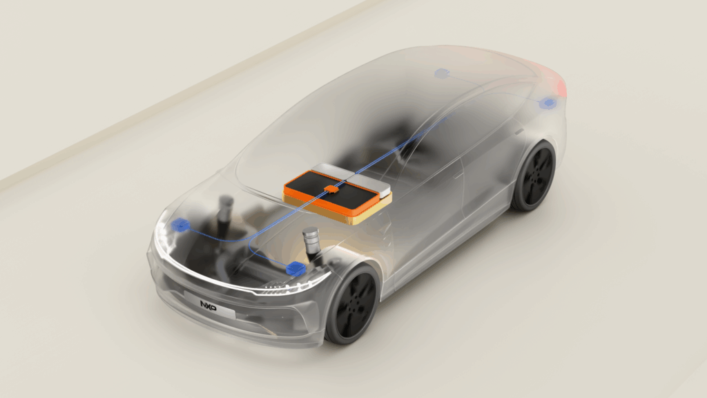
- Field Connectivity: Isolated I/O, CAN, RS-485, and Industrial Ethernet variants.
- Peripherals: ADCs/DACs, sensor conditioning, and storage expansion (M.2 NVMe).
Navigating Module Ecosystems and Standards
The choice of module standard dictates the routing discipline and mechanical constraints of your carrier board.
COM Express (Type 6 and Type 7)
Dominant in high-performance x86 applications. Type 6 focuses on general-purpose I/O with display support, while Type 7 is headless, leaning into multi-10GbE and server-grade throughput. These designs demand rigorous signal integrity (SI) and power integrity (PI) analysis due to their dense high-speed breakouts.
SMARC (Smart Mobility ARChitecture)
The go-to for low-power ARM and x86 systems. SMARC carriers often involve complex multimedia interfaces (MIPI CSI/DSI) and require careful thermal management within compact footprints.
OSM (Open Standard Module)
A newer, “solder-down” standard that eliminates the cost and profile of a physical connector. OSM carrier design requires advanced SMT assembly expertise and careful thermal dissipation strategies through the PCB itself.
Power Architecture and Sequencing
Power design is frequently the silent failure point of carrier boards. A “lab-stable” board often fails in the field because the input stage wasn’t designed for real-world harness transients.
The Input Stage
A production-grade input stage must include:
- Surge Suppression: Sized for energy dissipation, not just clamping voltage.
- Inrush Current Limiting: Essential for systems with significant bulk capacitance or hot-swap requirements.
- Reverse Polarity Protection: Utilizing low-RDS(on) MOSFETs to maintain efficiency.
Sequencing and Supervision
Embedded modules are sensitive to power-up/down timing. Carrier boards must implement supervisors that enforce known-good conditions before releasing the system reset. Failure to manage sequencing can lead to “back-powering” through I/O pins, which may cause latch-up or permanent silicon damage.
High-Speed Digital Design and Signal Integrity
As data rates push into Gen4 and Gen5 territory, the carrier board becomes a complex channel engineering project.
- Return Path Integrity: Differential pairs require a continuous reference plane. Any split in the plane under a high-speed route creates common-mode noise and EMI spikes.
- Impedance Control: This is a manufacturing outcome. You must lock your stack-up with your fabricator early to account for dielectric thickness and copper roughness.
- Via Engineering: At multi-gigabit speeds, vias are transmission line elements. Consider backdrilling or “teardrop” launches to minimize parasitic capacitance and stubs that cause resonance.
Design for EMC and Rugged Environments
EMC is not a final testing phase; it is a fundamental design constraint.
- Zoning: Physically separate noisy switching regulators and high-current loops from sensitive analog islands and clock distribution networks.
- Cable Egress: Treat the connector area as the primary EMC boundary. Use common-mode chokes at the entry points and ensure the RJ45 or USB shields are bonded correctly to the chassis or earth ground.
- Mechanical Retention: In high-vibration environments, rely on locking connectors and strain relief. Do not assume the module connector alone provides sufficient mechanical support.
Common Pitfalls in Carrier Board Development
- Ignoring DC Bias Derating: MLCC capacitors lose significant effective capacitance at their operating voltage. Always over-specify capacitance to ensure regulator stability.
- Underestimating Thermal Loads: A module might be rated for 15W, but the carrier-side PHYs, PoE controllers, and VRMs can easily add another 10W. Perform thermal simulation inside the final enclosure, not on an open bench.
- Inconsistent Shielding: Long, inductive pigtail grounds for cable shields often nullify the benefits of high-quality shielded connectors.
Closing Thoughts
Carrier board design is system engineering in PCB form. The most successful projects are those that prioritize the “boundaries”—the power entry, the connector launches, and the grounding philosophy. By getting these foundations right, the rest of the design becomes a matter of controlled execution rather than a cycle of troubleshooting.